Fermi Level In Intrinsic Semiconductor : Electronic Devices Fermi Energy Of An Intrinsic Semiconductor Youtube / Fermi level in intrinic and extrinsic semiconductors.
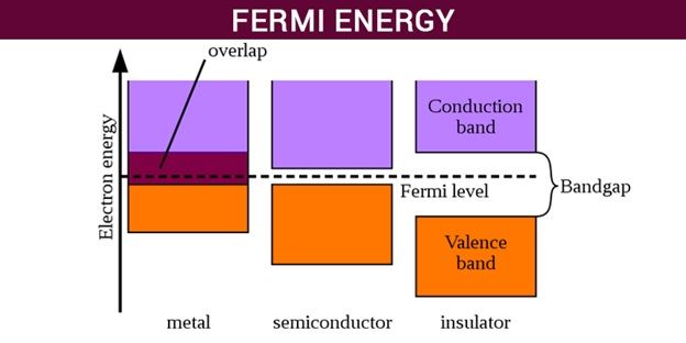
Fermi Level In Intrinsic Semiconductor : Electronic Devices Fermi Energy Of An Intrinsic Semiconductor Youtube / Fermi level in intrinic and extrinsic semiconductors.. Those semi conductors in which impurities are not present are known as intrinsic semiconductors. Карусель назад следующее в карусели. At any temperature above that it is very well defined and easy to. A donor level 0.25 ev above the top of the valence band, and an acceptor. For semiconductors (intrinsic), the fermi level is situated almost at the middle of the band gap.
In an intrinsic semiconductor, n = p. Therefore, the fermi level in an intrinsic semiconductor lies in the middle of the forbidden gap. Therefore, the fermi level for the intrinsic semiconductor lies in the middle of forbidden band. Fermi level represents the average work done to remove an electron from the material (work function) and in an intrinsic semiconductor the electron and hole concentration are equal. Room temperature intrinsic fermi level position).
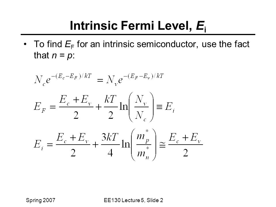
1 from In intrinsic semiconductors, the fermi energy level lies exactly between valence band and conduction band.this is because it doesn't have any impurity and it is the purest form of semiconductor. Distinction between conductors, semiconductor and insulators. (15) and (16) be equal at all temperatures, which yields the following expression for the position of the fermi level in an intrinsic semiconductor For an intrinsic semiconductor the fermi level is exactly at the mid of the forbidden band.energy band gap for silicon (ga) is 1.6v, germanium (ge) is 0.66v, gallium arsenide (gaas) 1.424v. $\begingroup$ intrinsic fermi level is considered at the center of the bandgap. Any way to know the fermi level just with the given information? Therefore, the fermi level in an intrinsic semiconductor lies in the middle of the forbidden gap. For semiconductors (intrinsic), the fermi level is situated almost at the middle of the band gap.
We know that si and ge have 4 valence electrons and these two elements possess properties like carbon because they are tetravalent.
Examining the consequences of fermi distribution in semiconductors. Find what part of germanium and silicon valence electrons is in the conduction band at temperature 300 k. Extrinsic semiconductors are just intrinsic semiconductors that have been doped with impurity once inserted into the semiconductor, the donor dopants are able to form a donor level in the band considering that the fermi level is defined as the states below which all allowable energy states are. An intrinsic semiconductor is one which is made of the semiconductor material in its extremely pure. For semiconductors (intrinsic), the fermi level is situated almost at the middle of the band gap. How many charge carriers does a sc have at temperature t? Differentiate between intrinsic semiconductors and intrinsic semiconductors? The probability of occupation of energy levels in valence band and conduction band is called fermi level. Fermi level for intrinsic semiconductor. An intrinsic semiconductor is an undoped semiconductor. Where is the fermi level within the bandgap in intrinsic sc? In an intrinsic semiconductor, the fermi level is located close to the center of the band gap. Hope it will help you.
Is the amount of impurities or dopants. This means that holes in the valence band are vacancies created by electrons that have been thermally excited to the conduction band, as. Therefore, the fermi level for the intrinsic semiconductor lies in the middle of forbidden band. Документы, похожие на «5.fermi level in itrinsic and extrinsic semiconductor». At absolute zero temperature intrinsic semiconductor acts as perfect insulator.
Fermi Energy And Fermi Level Definition Applications Formula from cdn1.byjus.com Where is the fermi level within the bandgap in intrinsic sc? The number of charge carriers is therefore determined by the properties of the material itself instead of the amount of impurities. And ni = intrinsic carrier concentration. Fermi level in intrinic and extrinsic semiconductors. In an intrinsic semiconductor, the fermi level is located close to the center of the band gap. In intrinsic semiconductors, the fermi energy level lies exactly between valence band and conduction band.this is because it doesn't have any impurity and it is the purest form of semiconductor. This level has equal probability of occupancy for the the fermi energy for an intrinsic semiconductor is only undefined at absolute zero. Assume that a particular defect in silicon introduces two discrete i ells:
In an intrinsic semiconductor, n = p.
Therefore, the fermi level for the intrinsic semiconductor lies in the middle of forbidden band. In semiconductors the fermi energy is close to the midpoint of the gap between the valence band and the conduction band. Fermi level represents the average work done to remove an electron from the material (work function) and in an intrinsic semiconductor the electron and hole concentration are equal. Differentiate between intrinsic semiconductors and intrinsic semiconductors? Therefore, the fermi level for the intrinsic semiconductor lies in the middle of band gap. Examining the consequences of fermi distribution in semiconductors. $\begingroup$ intrinsic fermi level is considered at the center of the bandgap. Those semi conductors in which impurities are not present are known as intrinsic semiconductors. (also, without looking up values from other sources). „ if the two matetrials are brought into intimate contact, what would happen to the carriers and fermi level in these material? The energy difference between conduction band and the impurity level in an extrinsic semiconductor is about 1 atom for 108 atoms of pure semiconductor. Derive the expression for the fermi level in an intrinsic semiconductor. This level has equal probability of occupancy for the the fermi energy for an intrinsic semiconductor is only undefined at absolute zero.
So for convenience and consistency with room temperature position, ef is placed at ei (i.e. Distinction between conductors, semiconductor and insulators. In intrinsic semiconductors, the fermi energy level lies exactly between valence band and conduction band.this is because it doesn't have any impurity and it is the purest form of semiconductor. An intrinsic semiconductor is one which is made of the semiconductor material in its extremely pure. A donor level 0.25 ev above the top of the valence band, and an acceptor.
Lecture 5 Outline Intrinsic Fermi Level Determination Of E F Degenerately Doped Semiconductor Carrier Properties Carrier Drift Read Sections 2 5 Ppt Download from images.slideplayer.com And ni = intrinsic carrier concentration. $\begingroup$ intrinsic fermi level is considered at the center of the bandgap. Fermi level in an intrinsic semiconductor. Is the amount of impurities or dopants. An intrinsic semiconductor is an undoped semiconductor. (15) and (16) be equal at all temperatures, which yields the following expression for the position of the fermi level in an intrinsic semiconductor Документы, похожие на «5.fermi level in itrinsic and extrinsic semiconductor». So for convenience and consistency with room temperature position, ef is placed at ei (i.e.
Assume that a particular defect in silicon introduces two discrete i ells:
Extrinsic semiconductors are just intrinsic semiconductors that have been doped with impurity once inserted into the semiconductor, the donor dopants are able to form a donor level in the band considering that the fermi level is defined as the states below which all allowable energy states are. However as the temperature increases free electrons and holes gets generated. (ii) fermi energy level : Therefore, the fermi level in an intrinsic semiconductor lies in the middle of the forbidden gap. Differentiate between intrinsic semiconductors and intrinsic semiconductors? Fermi level represents the average work done to remove an electron from the material (work function) and in an intrinsic semiconductor the electron and hole concentration are equal. Fermi level in intrinic and extrinsic semiconductors. A donor level 0.25 ev above the top of the valence band, and an acceptor. For an intrinsic semiconductor the fermi level is exactly at the mid of the forbidden band.energy band gap for silicon (ga) is 1.6v, germanium (ge) is 0.66v, gallium arsenide (gaas) 1.424v. At absolute zero temperature intrinsic semiconductor acts as perfect insulator. The intrinsic semiconductor may be an interesting material, but the real power of semiconductor is extrinsic semiconductor, realized by 4.6.3 relevance of the fermi energy. In an intrinsic semiconductor, n = p. Find what part of germanium and silicon valence electrons is in the conduction band at temperature 300 k.
Examining the consequences of fermi distribution in semiconductors fermi level in semiconductor. Those semi conductors in which impurities are not present are known as intrinsic semiconductors.


0 Komentar